Hubbard Radio Washington DC, LLC. All rights reserved. This website is not intended for users located within the European Economic Area.
Scientists at the Energy Department's National Renewable Energy Laboratory recently made a solar cell that comes close to the holy grail of 50% efficiency.
Best listening experience is on Chrome, Firefox or Safari. Subscribe to Federal Drive’s daily audio interviews on Apple Podcasts or PodcastOne.
Scientists at the Energy Department’s National Renewable Energy Laboratory recently made a solar cell that comes close to the holy grail of 50% efficiency. They’re using a technology known as multijunction. For more on the work and why it’s important, Federal Drive with Tom Temin spoke with senior scientist Myles Steiner. Read more here.
Interview transcripts:
Tom Temin: Dr. Steiner. Good, to have you on.
Dr. Myles Steiner: Thanks for having me.
Tom Temin: Tell us about this program that you’re working under. This is some way of getting to the next generation of solar cells, which I guess have not gotten more than 30 35% efficient,
Dr. Myles Steiner: Right. So we work under the Photovoltaics program, which is part of the Solar Energy Technology oOfice, which is itself part of EERE, so the Office of Energy Efficiency and Renewable Energy. And the PV program is looking at ways of developing low cost solar technology for domestic energy production. So we’re trying to figure out how to use solar energy to generate electricity for the American taxpayer.
Tom Temin: Yes, so this takes many forms. I mean, people put stuff on the roof that covers it with what looks like windows on top of roof. And then sometimes you’ll go by a field and you’ll see an acre of these kinds of panels. All of these use the similar technology and you’re trying to do what? Shrink it?
Dr. Myles Steiner: So most of those use silicon some of them used in films like cadmium telluride, what we are working on is a material system called three fives made from groups three and five of the periodic table. This would be a utility scale. So the kind of things we’re working on probably would not go on a typical homeowners house but would be part of a big field where you know, we you see trackers that are following the sun, so generating, you know, a lot of power that you could use to supply a whole neighborhood or whole city.
Tom Temin: So the purpose is to be able to do this with less surface area correct?
Dr. Myles Steiner: Well to do it with as high efficiency as possible. And the way we do it is we use optics to concentrate the lights, right, so instead of having a one square meter solar panel, you have an actual solar cell that’s maybe 100 times smaller, but you make up the intensity by putting on some kind of lens and you may have seen some of these listeners may have seen some of these in pictures or driving around, you have big mirrors that focus light onto a solar cell or a lens that focuses down onto a solar cell. And so in that way, you can use a lot less semiconductor material.
Tom Temin: Got it in the elements that you’re working with, then are themselves sensitive to light, and they produce some sort of current. And tell us about the idea of six junction, or this is a multi layer type of approach. What is it you’re trying to engineer here?
Dr. Myles Steiner: So the idea here is to span as wide a range of the solar spectrum as possible, and to do it with as few losses as possible. So in a silicon solar cell picks up about half the solar spectrum, and that’s just because of where its bandgap is situated. In other words, it can absorb light that is above its bandgap. Bandgap is sort of a characteristic energy of the semiconductor. But that means you lose a lot of photons because they’re not absorbed by the semiconductor. So what we’re trying to do is create a structure that spans a very wide range of the solar spectrum absorb all that light. And then the six junction part of it is that we divide up that spectrum into smaller bins. And each junction or each mini solar cell, if you will, is tuned to a narrower range of the solar spectrum. And so you know, a junction is just, you can think of it as a solar cell, it’s really a diode that’s formed of two different semiconductors with different electrical properties that we stack the one on top of each other. And so the top junction absorbs the highest energy light, you know, the blue light, if you will, and then the next junction absorbs slightly lower energy, longer wavelength, light, and so on all the way into the infrared.
Tom Temin: So each layer passes what it doesn’t take on to the next layer, so to speak?
Dr. Myles Steiner: Right, each junction passes what it doesn’t take. I would say that there are about 140 actual layers in our structure. So each junction is formed from quite a few individual semiconductor layers. It’s a pretty complex structure.
Tom Temin: And just out of curiosity, these are manufactured like semiconductor so circuits with deposition?
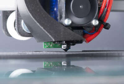
Dr. Myles Steiner: Yeah, we deposit them by a technique called metal organic vapor phase epitaxy. It’s a growth technique where you flow gases of chemicals at high temperature and the gas is paralyzed, and the tonic species of interest land on a surface that you’re growing on. So we do that in a deposition chamber at NREL. There’s other kinds of deposition chambers out there that make these kinds of solar cells and, of course, other kinds of growth techniques.
Tom Temin: And this is something that the industry has not done for itself. I guess my question maybe is, you’re doing science or engineering here?
Dr. Myles Steiner: We’re doing both. We’re certainly engineering a structure that converts a lot of light into electricity, but there’s a tremendous amount of material science and device physics on the material science side. You know, one of the ways that we are able to span the solar spectrum is by creating materials that have a different crystal structure than The material on which they’re grown. So we grow it on a gallium arsenide substrate. And we purchase a wafer of gallium arsenide from manufacturer. And then we deposit the layers of the semiconductor, one on top of each other. But at some point we get to alloys that have a larger lattice constant than the gallium arsenide. And we have to do that in order to make alloys that have a lower bandgap. And there’s a tremendous amount of material science and learning how to change the lattice constant in a way that maintains really good material quality. If you have poor material quality, you end up with a very bad solar cell. And we have learned over the past 20 years to grow these materials with really good material quality, even though we’re changing the crystal structure.
Tom Temin: And at some point, this has to be manufacturable at scale, I imagine?
Dr. Myles Steiner: Well, that would be the goal. These three five solar cells are widely used in the satellite industry. And there are a number of American companies that manufacture these, there’s some international companies as well that manufacture three five solar cells. So there’s already a bit of a manufacturing base for this technology from The satellite industry, you know, learning how to do this at scale for domestic energy production is a bit of a different story. There have been some commercial efforts to do this over the past 20 years, there are a few power plants around the United States. There’s one in Colorado, for example, that generates about 30 megawatts that have started to commercialize some of these kinds of technology.
Tom Temin: It sounds like with these various elements, each seeing a different part of the spectrum, that the solar cells could give off substantial power when it’s cloudy?
Dr. Myles Steiner: So actually, that’s not true. And the reason is that because the concentration is very high, you have to track the sun, right? You have to follow the sun exactly. And that means you don’t pick up a lot of diffuse lights, right. So your your, instead of a if you think of a silicon solar panel on your roof, it picks up light from, you know, from a whole hemisphere above the solar cell. But if you put a concentrator lens in front of it, you you now really only pick up light that’s very narrowly focused on the sun itself.
Tom Temin: It’s like trying to light a match with a magnifying glass. You have to have the sun out.
Dr. Myles Steiner: Yes, right, exactly. If you tilt the magnifying glass away from the match, you lose everything.
Tom Temin: And does the lab have a process for getting this learning into the commercial stream? At some point?
Dr. Myles Steiner: Yeah, we’ve worked with companies to transfer technology. Our group has been around for 30 years. We pioneered this before my time, but scientists who started our group pioneered the multi junction solar cell that now flies on satellites, and we have a really good track record of technology transfer through licensing agreements. You know, more recently, we have worked with companies on aspects of our technology for this project and for other projects. So you know, there’s a well trodden path to technology transfer here. You know, of course, we publish papers at conferences and journals and companies will read those and so even if we don’t have a formal agreement, they’ll they’ll sometimes pick up some of the things we’ve learned.
Tom Temin: And I’ve seen, you know, Colorado light can be pretty intense, it can be a very sunny state. Are you one of those people that has solar sails on your own roof?
Dr. Myles Steiner: I wish I could say yes, but unfortunately, we have a big tree on the western side of our house which shades the roof for a decent fraction of the afternoon. And our roof also doesn’t really face out. So, not our house.
Tom Temin: A true environmentalist dilemma, I guess, the tree or the sunshine.
Dr. Myles Steiner: You know, when we purchased our house, we looked for location and several other things and solar was on there.
Tom Temin: Myles Steiner is a senior scientist at the National Renewable Energy Laboratory in Golden, Colorado. Thanks so much for joining me.
Dr. Myles Steiner: Thanks for having me. Appreciate it.
Copyright © 2024 Federal News Network. All rights reserved. This website is not intended for users located within the European Economic Area.
Tom Temin is host of the Federal Drive and has been providing insight on federal technology and management issues for more than 30 years.
Follow @tteminWFED